- 您现在的位置:买卖IC网 > Sheet目录2007 > MAX107ECS+ (Maxim Integrated Products)IC ADC 6BIT 400MSPS DL 80-TQFP
MAX107
Dual, 6-Bit, 400Msps ADC with On-Chip,
Wideband Input Amplifier
_______________________________________________________________________________________
3
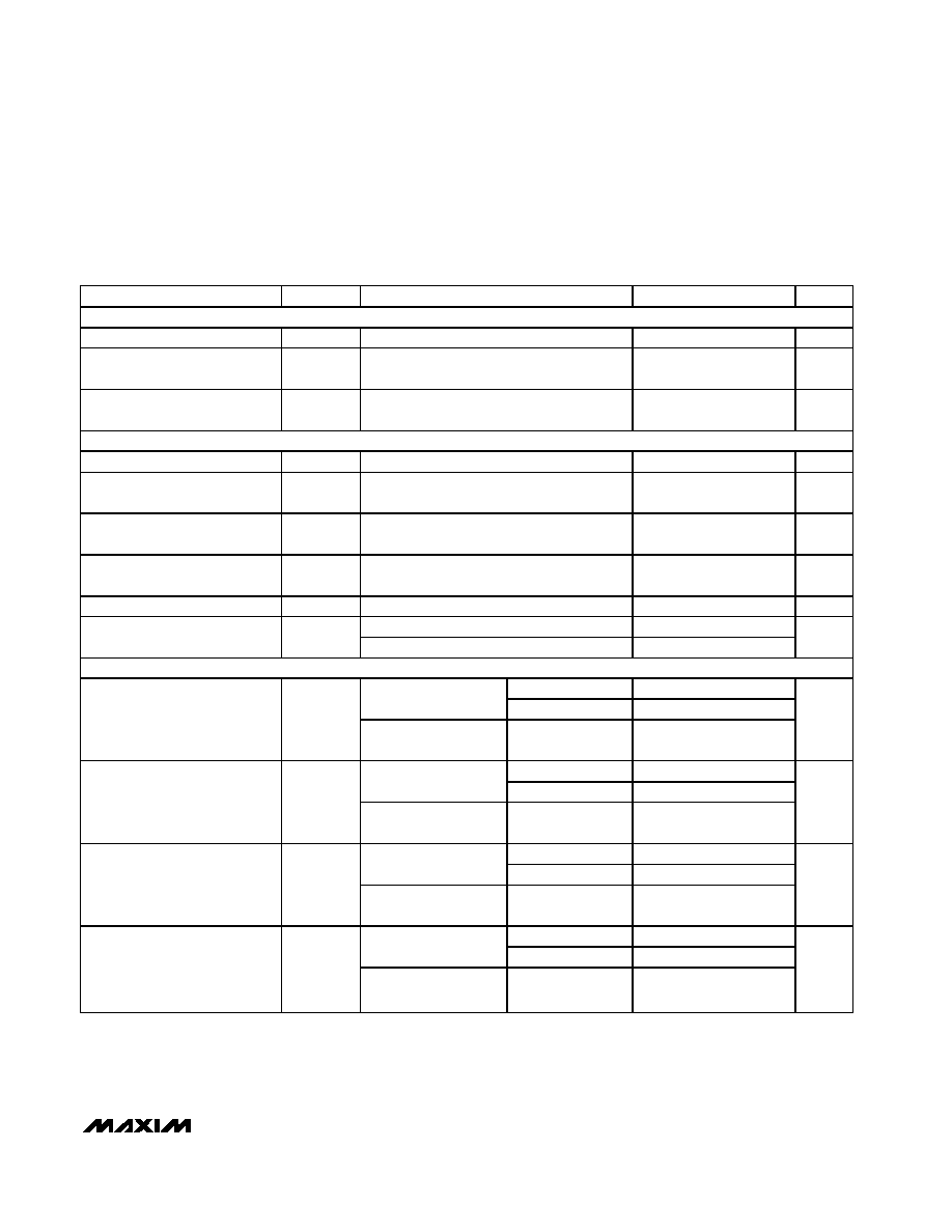
ELECTRICAL CHARACTERISTICS (continued)
(AVCC = AVCCI = AVCCQ = AVCCR = +5V, OVCCI = OVCCQ = +3.3V, AGND = AGNDI = AGNDQ = AGNDR = 0, OGNDI = OGNDQ
= 0, fCLK = 401.408MHz, CL = 1F to AGND at REF, RL = 100
±1% applied to digital LVDS outputs, TA = TMIN to TMAX, unless
otherwise noted. Typical values are at TA = +25
°C)
PARAMETER
SYMBOL
CONDITIONS
MIN
TYP
MAX
UNITS
CLOCK INPUTS (CLK+, CLK-)
Clock Input Resistance
RCLK
CLK+ and CLK- to AGND
5
k
Clock Input Resistance
Temperature Coefficient
TCRCLK
150
ppm/
°C
Minimum Clock Input
Amplitude
500
mVp-p
LVDS OUTPUTS (P0I
± TO P5I±, P0Q± TO P5Q±, A0I± TO A5I±, A0Q± TO A5Q±, DREADY+, DREADY-, DOR+, DOR-)
Differential Output Voltage
VOD
247
400
mV
Change in Magnitude of
VOD
Between “0” and “1” States
VOD
±25
mV
Steady-State Common Mode
Output Voltage
VOC(SS)
1.125
1.375
V
Change in Magnitude of VOC
Between “0” and “1” States
VOC
±25
mV
Differential Output Resistance
80
160
Short output together
2.5
Output Current
Short to OGNDI = OGNDQ
25
mA
DYNAMIC SPECIFICATION
Differential
5.4
5.9
fIN = 124.999MHz at
-0.5dB FS (Note 9)
Single-ended
5.9
Effective Number of Bits
(Note 8)
ENOB
fIN = 200.067MHz at
-0.5dB FS
Differential
5.75
Bits
Differential
35
37
fIN = 124.999MHz at
-0.5dB FS (Note 9)
Single-ended
37
Signal-to-Noise Ratio
(Notes 10, 11)
SNR
fIN = 200.067MHz at
-0.5dB FS
Differential
36.6
dB
Differential
-49.5
-42
fIN = 124.999MHz at
-0.5dB FS (Note 9)
Single-ended
-49.5
Total Harmonic Distortion
(Note 11)
THD
fIN = 200.067MHz at
-0.5dB FS
Differential
-44.5
dBc
Differential
43
51
fIN = 124.999MHz at
-0.5dB FS (Note 9)
Single-ended
51
Spurious-Free Dynamic Range
SFDR
fIN = 200.067MHz at
-0.5dB FS
Differential
45.5
dB
发布紧急采购,3分钟左右您将得到回复。
相关PDF资料
MAX1080AEUP+
IC ADC 10BIT 400KSPS 20-TSSOP
MAX1084AESA+
IC ADC 10BIT 400KSPS 8-SOIC
MAX1093AEEG+
IC ADC 10BIT 250KSPS 24-QSOP
MAX1098CEAE+
IC ADC 10BIT SERIAL 16-SSOP
MAX11040GUU+T
IC ADC 24BIT 4CH 38-TSSOP
MAX11046ECB+T
IC ADC 16BIT PAR 250KSPS 64TQFP
MAX11046ETN+T
ADC 16BIT SAMPLING 8CH 56-TQFN
MAX11049ECB+
IC ADC 16BIT PAR 250KSPS 64TQFP
相关代理商/技术参数
MAX107ECS+T
功能描述:模数转换器 - ADC Dual 6-Bit 400Msps w/OnChip Wdbnd InAmp RoHS:否 制造商:Texas Instruments 通道数量:2 结构:Sigma-Delta 转换速率:125 SPs to 8 KSPs 分辨率:24 bit 输入类型:Differential 信噪比:107 dB 接口类型:SPI 工作电源电压:1.7 V to 3.6 V, 2.7 V to 5.25 V 最大工作温度:+ 85 C 安装风格:SMD/SMT 封装 / 箱体:VQFN-32
MAX107ECS-D
功能描述:模数转换器 - ADC RoHS:否 制造商:Texas Instruments 通道数量:2 结构:Sigma-Delta 转换速率:125 SPs to 8 KSPs 分辨率:24 bit 输入类型:Differential 信噪比:107 dB 接口类型:SPI 工作电源电压:1.7 V to 3.6 V, 2.7 V to 5.25 V 最大工作温度:+ 85 C 安装风格:SMD/SMT 封装 / 箱体:VQFN-32
MAX107ECS-TD
功能描述:模数转换器 - ADC RoHS:否 制造商:Texas Instruments 通道数量:2 结构:Sigma-Delta 转换速率:125 SPs to 8 KSPs 分辨率:24 bit 输入类型:Differential 信噪比:107 dB 接口类型:SPI 工作电源电压:1.7 V to 3.6 V, 2.7 V to 5.25 V 最大工作温度:+ 85 C 安装风格:SMD/SMT 封装 / 箱体:VQFN-32
MAX107EVKIT
功能描述:数据转换 IC 开发工具 RoHS:否 制造商:Texas Instruments 产品:Demonstration Kits 类型:ADC 工具用于评估:ADS130E08 接口类型:SPI 工作电源电压:- 6 V to + 6 V
MAX108
制造商:MAXIM 制造商全称:Maxim Integrated Products 功能描述:【5V, 1.5Gsps, 8-Bit ADC with On-Chip 2.2GHz Track/Hold Amplifier
MAX1080
制造商:MAXIM 制造商全称:Maxim Integrated Products 功能描述:300ksps/400ksps, Single-Supply, Low-Power, 8-Channel, Serial 10-Bit ADCs with Internal Reference
MAX1080ACUP
功能描述:模数转换器 - ADC RoHS:否 制造商:Texas Instruments 通道数量:2 结构:Sigma-Delta 转换速率:125 SPs to 8 KSPs 分辨率:24 bit 输入类型:Differential 信噪比:107 dB 接口类型:SPI 工作电源电压:1.7 V to 3.6 V, 2.7 V to 5.25 V 最大工作温度:+ 85 C 安装风格:SMD/SMT 封装 / 箱体:VQFN-32
MAX1080ACUP+
功能描述:模数转换器 - ADC Low-Power 8-Ch 10-Bit w/Int Ref RoHS:否 制造商:Texas Instruments 通道数量:2 结构:Sigma-Delta 转换速率:125 SPs to 8 KSPs 分辨率:24 bit 输入类型:Differential 信噪比:107 dB 接口类型:SPI 工作电源电压:1.7 V to 3.6 V, 2.7 V to 5.25 V 最大工作温度:+ 85 C 安装风格:SMD/SMT 封装 / 箱体:VQFN-32